|
|
|
Categories
|
|
Information
|
|
Featured Product
|
|
|
 |
|
|
There are currently no product reviews.
 ;
This service Manual for my JVC AV29BF10EES is very helful. Everything is show in detailed diagrams!!!! If you need really good source of information for this type JVC you are on the right place. I am satisfied and very glad for this excellent book. Thank you.
;
Great service, great value like always!!!
Some of the writing is a bit blur but all is usable.
A+++++++++++++++++
;
Great service manua!
Always great value and fast service A++++++++++++++++++
;
Excellent Service manual, good quality scans, quick service and very good value. Well reccomended ! All good.
;
Great value service manual!
Good-quality scans. Detailed and valuable informations.
A+++++++++++++++
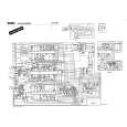
IC, LC75374E Pin No.
1 2
Pin Name
RVR IN R COM
I/O
I �
Description
4dB volume control input. Must be driven at a low impedance. 1dB volume control common pin. (Connected to GND through a capacitor) For the connection of capacitors that compensate for bass and treble in the tone control circuits.
3~5
RT1 ~ RT3
�
A high-frequency compensation capacitor must be connected between RT1 and RT2. A low-frequency compensation capacitor must be connected between RT2 and RT3.
6 7 8 9 10 11 12 13 14 15 16 17 18
RT OUT RS IN NC NC RS3
O I � � O
Tone control output. Super bass input. Must be driven at a low impedance. Connected to GND. Not connected. For the connection of RCH super bass compensation capacitors. Fader input. Must be driven at a low impedance. Fader output. The front and rear sides can be attenuated independently. GND. Serial data and clock input for control. Chip enable. Data is written in the internal latch when the chip enable signal goes "L" from "H", and each analog switch is activated. Data transfer is enabled at "H". Generates a 1/2VDD power source. A capacitor must be connected between VREF and GND as a troubleshooting against power ripples. Fader output. The front and rear sides can be attenuated independently. Fader input. Must be driven at a low impedance. For the connection of LCH super bass compensation capacitors. Not connected. Connected to GND. Super bass input. Must be driven at a low impedance. Tone control output. For the connection of capacitors that compensate for bass and treble in the tone control circuit.
RS OUT FR IN FR OUT O RR OUT VSS CL I DI CE � � I
19 20 21 22 23 24 25 26 27 28
VREF RL OUT
�
O FL OUT FL IN LS OUT O LS3 NC NC LS IN LT OUT � � I O I
29 ~ 31
LT3 ~ LT1
A high-frequency compensation capacitor must be connected between LT1 and LT2. A low-frequency compensation capacitor must be connected between LT2 and LT3.
32 33 34 35 36 37 38 39
L COM LVR IN LSELO AUX (L) CD (L)
� I O
1dB volume control common pin. 4dB volume control input. Must be driven at a low impedance. Input selector output pin.
I TUN (L) TP (L) VDD �
Signal input pins.
Power supply.
� 25 �
 $4.99 CDCMP32 AIWA
Owner's Manual Complete owner's manual in digital format. The manual will be available for download as PDF file aft…
|
|
|
> |
|