|
|
|
Categories
|
|
Information
|
|
Featured Product
|
|
|
 |
|
|
There are currently no product reviews.
 ;
An excellent document to assist in the repair of my old personal tape player. It includes full circuit diagrams and physical layout drawings and full instructions on disassembly and fault finding.
Well worth the meagre price.
;
Very good conversation, Pretty fast Service, wood do it again,
Have paid by Paypal, so i got the Service Manual online after 15 Min.
Very helpfully.
Greeting from Germany,
Hans
;
Good-quality scans. Detailed description. I hope I can repair the machine.
;
High-quality scanning. Detailed description. Recommend for all technician. A+++
;
This is a good quality scan of the original Service Manual from Nordmende, Germany. Contains the circuit diagram, PCB layout, adjust/tune instructions as well. It is NOT in English but in GERMAN language! That was quite right for my german friend from the lower east side in Berlin.
CIRCUIT DESCRIPTION
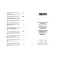
Setting the batteries or AC adaptor (see figure 7) When setting the batteries or AC adaptor, the voltage VDD2 is always applied to RAM and CPU since Q6 and IC5 are turned on. Power on sequence (see figure 7) When the power switch is turned on, PON signal is being H (PON = VDD2). CPU knows to turn the power switch on, it provides H from VCON terminal to base of transistor Q4. Then both transistors Q4 and Q3 are turned on, the voltage VDD1 is applied to all devices. Power off sequence (see figure 7) When the power switch is turned off, POFF signal is being H(POFF= VDD2). CPU knows to turn the power switch off, VCON signal and base of Q4 will be L. Then both transistors Q4 and Q3 are turned off, Q3 stops to supply the voltage VDD1. Power down sequence (see figure 7) If the voltage across the batteries lowers and the terminal DPW of CPU comes less than 4.5V, VCON signal is L. Then both transistors Q4 and Q3 are turned off, Q3 stops to provide the voltage VDD1. Print sequence (see figure 7) When the PRINT button is pressed, TCON signal is H. Then both transistors Q2 and Q1 are turned on, the voltage VP for printing will be 9V.
Q1 Fuse
8.6V 8.8V 8.4V 0V 8.6V 8.8V 0V 0V 5.0V 4.8V
IC5
5.0V 4.8V
VP (+9 V) VDD2 (+5 V)
Q3
4.8V 0V
8.4~0V 8.4~0V
VDD1 (+5 V)
+
8.6V 8.8V 0V 0V 0V 0V
4.2V 4.8V
+
0V 4.8V 4.8V 0V
Q2
Q4
0V 0V
GND
VDD1
VCON DPW IC1 PON VDE TCON ON POFF
CPU
OFF
Power Switch Note : The voltages around transistors mean as follows; Upper figure : Power ON at no operation. Lower figure : Power OFF. Figure-7
�5�
|
|
|
> |
|