|
|
|
Categories
|
|
Information
|
|
Featured Product
|
|
|
 |
|
|
There are currently no product reviews.
 ;
This service Manual for my JVC AV29BF10EES is very helful. Everything is show in detailed diagrams!!!! If you need really good source of information for this type JVC you are on the right place. I am satisfied and very glad for this excellent book. Thank you.
;
Great service, great value like always!!!
Some of the writing is a bit blur but all is usable.
A+++++++++++++++++
;
Great service manua!
Always great value and fast service A++++++++++++++++++
;
Excellent Service manual, good quality scans, quick service and very good value. Well reccomended ! All good.
;
Great value service manual!
Good-quality scans. Detailed and valuable informations.
A+++++++++++++++
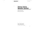
SRS-Z750/Z750PC SECTION 2 DIAGRAMS
2-1. PRINTED WIRING BOARD (SRS-Z750) 2-2. SCHEMATIC DIAGRAM (SRS-Z750)
Note: � All capacitors are in µF unless otherwise noted. pF: µµF 50 WV or less are not indicated except for electrolytics and tantalums. � All resistors are in � and 1/4 W or less unless otherwise specified. � C : panel designation. � U : B+ Line. � Power voltage is dc 15 V and fed with regulated dc power supply from external power voltage jack. � Voltage is dc with respect to ground under no-signal condition. � Voltages are taken with a VOM (Input impedance 10 M�). Voltage variations may be noted due to normal production tolerances. � Signal path. F : AUDIO
� IC Block Diagram IC1 LA4663
RIPPLE FILTER/ STARTING TIME 1 IN1 2 PRE GND 3 INPUT AMP + � OUTPUT AMP
IN2 4 STANDBY 5
+ � INPUT AMP
OUTPUT AMP
� Semiconductor Location
Ref. No. D1 D2 D3 D4 IC1 Q1 Q2 Location D-2 D-3 F-2 F-2 D-2 E-3 E-3 Note: � X : parts extracted from the component side. � Y : parts extracted from the conductor side. � b : Pattern from the side which enables seeing.
SIGNAL MUTE VCC1 VCC2 +OUT2 POWER GND2 �OUT2 �OUT1 POWER GND1 +OUT1
6 7 8 9 10 11 12 13 14
�3�
�4�
|
|
|
> |
|