|
|
|
Categories
|
|
Information
|
|
Featured Product
|
|
|
 |
|
|
There are currently no product reviews.
 ;
let's say first that i do not need to have a credit for my opinion, i am a retired sparkie and i voluteerd to fix an electronic device for a local "Youthgroup",as no diagram was present i checked the "net" and gambled on this site and paying some fee via PayPall, i was gladly surprised that the manual arrived as was stated, GOOD SHOW, and best wishes, John
;
I had been looking for a Manual for my CS2150 for quite a while -- in fact I had just about given up. I saw this site and decided to download the Manual. When I Received it by Email I was really pleased with what I got, with the result that My Kenwood 'Scope is now 100% repaired and working well. As an AV Serviceman, you need a good 'scope, and thanks to this site, and the Service Manual, I have been able to repair it. The Manual was a copy of the Factory Original and the copy was very clear, especially in the area of the Circuit Schematics, where You really need to be sure of what You are looking at.
;
I recently purchased a manual for a Samsung DLP tv to help with a trouble shooting problem I was having. Every tv repair shop wanted close to $400.00 for the fix, but after I found Owner-Manuals.com I hit pay dirt. The manual they had for me to purchase and download was a complete service manual for the exact tv I needed. It was complete with wiring diagrams, schematics, and even part numbers. If your the fix it yourself type I highly recommend trying to find any manual here before paying someone else to fix whatever problem your having.
;
Once again, excellent price and manual delivered in a timely manner and as advertised!
;
Outstanding quality manual. This is the exact documentation I needed to service my AKAI GX-210D. This is a PERFECT COPY of the service manual for my machine. Outstanding service. Thank-you!
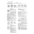
SECTION 3 DIAGRAMS
3-1. CIRCUIT BOARDS LOCATION
THIS NOTE IS COMMON FOR PRINTED WIRING BOARDS AND SCHEMATIC DIAGRAMS. (In addition to this, the necessary note is printed in each block.) For schematic diagrams.
Note: � All capacitors are in µF unless otherwise noted. pF: µµF 50 WV or less are not indicated except for electrolytics and tantalums. � All resistors are in � and 1/ 4 W or less unless otherwise
WAVEFORM 1
3.8Vp-p
4MHz
IC902 1 XOUT
PS board
OUTLET board
SP-TM board
specified. � ¢ : internal component. � 2 : nonflammable resistor. � 5 : fusible resistor. � C : panel designation. Note: The components identified by mark ! or dotted line with mark ! are critical for safety. Replace only with part number specified.
SIRCS board PHONO board
� � � �
SIRCS SUB board
HP board
U : B+ Line. V : B� Line. H : adjustment for repair. Voltages and waveforms are dc with respect to ground under no-signal (detuned) conditions. no mark : POWER ON � Voltages are taken with a VOM (Input impedance 10 M�). Voltage variations may be noted due to normal production tolerances. � Waveforms are taken with a oscilloscope. Voltage variations may be noted due to normal production tolerances. � Circled numbers refer to waveforms. � Signal path. F : TUNER
SP-SW board
INPUT board MAIN board VOL board
PANEL board
For printed wiring boards.
Note: � X : parts extracted from the component side. � Y : parts extracted from the conductor side. � b : Pattern from the side which enables seeing.
� Indication of transistor
BC E These are omitted
�5�
�6�
|
|
|
> |
|