|
|
|
Categories
|
|
Information
|
|
Featured Product
|
|
|
 |
|
|
There are currently no product reviews.
 ;
Good quality (clearly readable) manual, I'm glad I could find it here, at a bargain price!
;
Speedy transaction with a quick download. Awesome hassle-free service.
;
very poolite and healpful secure transaction thanks allot
;
- Very good scan quality, PERFECT!
- Sehr gute scan Qualitaet, empfehlenswert!
Wolfgang Sundhaus
 ;
Good site, works ok and you get what you order, no problems experienced, got my manual within a day. A++++
Philips Semiconductors
100 � 450 MHz 250 W Power Ampli�er with the BLF548 MOSFET
Application Note AN98021
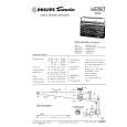
In order to compensate for the 6 dB/octave slope, matching to Zin is achieved at 450 MHz. At lower frequencies a mismatch is created, resulting in a decrease of powergain inversely proportional to the increase of the gain related to the transistor�s 6 dB/octave slope. The network listing of the input circuitry, again presented as a 3-port, is given in �Appendix B�. The network response (both input returnloss and predicted powergain) is given in Fig.4. Finally the schematic diagram and list of components are given in Fig.5. The unit�s layout is given in Fig.6. Note: two toroidal cores around T2 and T3 are used to prevent oscillations. 5 5.1 ADJUSTMENT OF THE AMPLIFIER Tuning the outputnetwork
In order to terminate the transistor with the proper load impedance, first the output network has to be tuned. The transistor was replaced by a dummyload, representing the transistors output impedance under full power conditions. The dummyload was realized after fitting the data of Table 3. To the dummyload model (roughly Rload in parallel with Coss, in series with draininductance Ld). Later the model was compensated for parasitics of both SOT262 header and network components. Initial settings for each side of the dummyload are: Rload = Vds2/2 � Pl = 5.2 � C = 1.15 � Coss = 104 pF L = Ld = 0.5 nH The network listing is given in �Appendix C�. The final result, the dummyload lay-out, is given in Fig.7.
handbook, halfpage
20
MGH787
(1)
10
0
(2)
�10
�20 100
200
300
400 500 frequency (MHz)
(1) DB [S12]. (2) DB [S22].
Fig.4 Simulated network response of inputside (predicted Gp = f(f)).
1998 Mar 23
9
|
|
|
> |
|