|
|
|
Categories
|
|
Information
|
|
Featured Product
|
|
|
 |
|
|
There are currently no product reviews.
 ;
A complete manual with all the needed details of calibrations and service instructions about the radio receiver.
A big deal.
Many thanks !
;
Fast delivery and good quality copy. To be recommended
;
Excellent product, very clear print. Detailed circuit and assembly diagrams - this enabled me to repair my CD player with confidence. I highly recommend this site.
;
Fast access, 100% correct and complete service manual
;
just what i was seeking .had a password issue but the review allowed me to circumvent and download was great
TK-3130/3131
CIRCUIT DESCRIPTION
PLL System
s VCO Circuit
The VCO is housed in a shield case. The VCO circuit consists of a transistor (Q4), a variable capacity diode (D4) for frequency control, a variable capacity diode (D8) for modulation, transmit/receive frequency shift diode (D17), control transistor (Q2), variable capacitor (TC1) for PLL lock voltage control, and oscillator buffer amplifier (Q5).
R11 LV
C198 R36 C38 R17 D8 C194 C27
In receive mode, the shift signal T/R goes low, Q2 turns off, and the shift diode (D17) not contact. Q4 produces the first local frequency for reception. (Receive channel frequency � 38.85MHz) In transmit mode, the shift signal T/R goes high, Q2 turns on and D17 does conducts. Q4 produces about 460~470 MHz and the VCO frequency equals the transmit channel frequency. The 3.0V circuit voltage is produced by ripple removing filter circuit Q3.
C41 Q4 C45 Q5
R126 L9
R35 L44
C186 D17
L8 C185
R25
VCO OUT
L43 D4 TC1 C36
C33
C42
T/R
R14 R146
R21
R18
L11 Q3
C32
R10
C29
D3 R24 L10
R23 R22
C46
+ Q2 MOD 3C
R15 C44
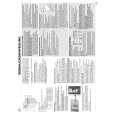
Fig. 7 VCO circuit
s PLL Circuit
Frequency data is sent to the PLL IC (IC1) from the CPU (IC204) as serial data when the power turns on, when the channel is changed, or when transmission begins. It sets the variable divider in the PLL IC. The TCXO (X1) produce a 12.8MHz reference frequency. It is divided to produce a 12.5kHz PLL comparison frequency in the PLL IC. The VCO input is divided by the divide ratio set by the divider in the PLL IC to generate 12.5kHz. It is compared with the reference comparison frequency by the phase comparator to detect a phase difference. The charge pump circuit in the PLL IC converts it to a control voltage that can drive the VCO directly. The control voltage passes through a loop filter which passes low frequency and is applied to the VCO control pin to control the oscillator frequency. The loop filter removes unwanted harmonics and noise contained in the output from the phase comparator and determines PLL response and synchronizing characteristics by the amplitude and phase characteristics (Fig. 8).
s Unlock Detection Circuit
If the PLL cannot be synchronized for some reason or other when switching the channel or changing between transmission and reception, the PLL IC outputs a low unlock detection signal. This signal goes to the CPU to inhibit transmission when the PLL is unlocked.
X1 12.8MHz CP1 + + + 3C Loop filter LV VCO F OUT FIN1 PLL IC IC1 LD STB DATA CK 3C CPU (IC204) UL PLL data (CPU) XIN TCXO TO Vcont
3C,T/R,MOD VCO OUT
Fig. 8
PLL circuit
C31 C30 R26 L12
7
|
|
|
> |
|