|
|
|
Categories
|
|
Information
|
|
Featured Product
|
|
|
 |
|
|
There are currently no product reviews.
 ;
Good quality service manual.It has helped me to fix my FV1800,particularly for replacing the dial cord.The scheme is on A3 format and very readable.Thank.Olivier.
;
This manual is complete and very readable.It was a great help for my two ICF5800L.The first one had the dial cord broken,and without the service manual it is impossible to replace it.Thank.Olivier.
 ;
This is a top quality manual. You couldn't get better if you had the original and scanned it yourself. Best price on the net as well. Diagrams are clear and complete, text is sharp and easy to read. Granted you don't get the manual the second you click pay, but the few hours you have to wait for it to be available for download isn't a problem at all. This is a very reliable company.
Very VERY pleased with the product, and will buy others. Thanks!
;
In a word AWESOME.
I never expected the quality and abundant content that I got with this manual. Everything you'd ever want to know from a service perspective is found in this manual, along with... as a bonus, operating instructions on how to use the unit. WOW. Very impressed with the quality of the manual. You won't be disappointed if you're looking for the EVS900 service manual.
;
I thank Owen-Manuals.com for the wonderful service rendered to me, and this manual which I purchased helped me a lot in servicing my Denon System, which was lying in a dead state.
Thanks Owner-Manual.com
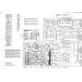
PT-11 Chassis Service Manual
SOUND IF CIRCUIT
On mono models;
The sound bandpass and trap filters have to be connected externally. The filtered intercarrier signal is fed to a limiter circuit and is demodulated by means of PLL demodulator. The PLL circuit tunes itself automatically to the incoming signal, consequently, no adjustment is required. The volume is DC controlled. The composite audio output signal has an amplitude of 700 mV RMS at a volume control setting of -6 dB. The de-emphasis capacitor has to be connected externally. The non-controlled audio signal can be obtained from pin 1 via a buffer stage. The amplitude of this signal is 350 mV RMS. The TDA8362 external audio input signal must have an amplitude of 350 mV RMS. The audio/video switch is controlled via the chrominance input pin.
On stereo models;
On stereo models, the adjustable sound output pin (pin50) is used for mono sound. An external sound IF circuit TDA3845 is used for NICAM B/G, I stereo systems. For NICAM L stereo system, TDA4470B Sound IF IC is used so that obtain AM sound and NICAM I sound carrier. On German Stereo system, TBA120U is used as FM demodulator for second sound carrier.
SYNCHRONIZATION
CIRCUIT
The sync separator is preceded by a voltage controlled amplifier which adjusts the sync pulse amplitude to a fix level. The sync pulses are then fed to the slicing stage (separator) which operates at 50 % of the amplitude. The separated sync pulses are fed to the first phase detector and to the coincidence detector. The coincidence detector is used for transmitter identification and to detect whether the line oscillator is synchronized. When the circuit is not synchronized, the voltage on the peaking control pin (pin 14) is LOW so that this condition can be detected externally The IC TDA8362 contains a start up circuit for the horizontal oscillator. When this feature is required a current of 6.5 mA has to be supplied to pin 36.
COLOR DECODING
TDA8362 contains PAL and NTSC decoder (TDA8361 contains only PAL decoder) but it can cooperate with the secam add-on secam decoder TDA8395. The communication between two IC�s is achieved via pin 32. The TDA8362 supplies the reference signal (4.43 MHz) for the calibration system of the TDA8395, identification of the color standard is via the same connection. When a SECAM signal is detected by the TDA8395 the IC will draw a current of 150 uA. When TDA8362 has not identified a color signal in this condition it will go into the SECAM mode, that means it will switch of the R-Y and B-Y outputs and increase voltage level on pin 32.
41 VERTICAL
DEFLECTION
CIRCUIT
WITH TDA3653B
The TDA3653B is vertical deflection circuit for drive of various deflection systems with currents up to 1.5 A peak to peak. Pin 5 is the output pin. the supply for the output stage is fed to pin 6 and the output stage ground is connected to pin 4. Pin 1 is the input for the driver of the output stage . The signal at pin 1 is also applied via external resistors to pin 3 which is the input of the switching circuit. When the flyback starts, this switching circuit rapidly turns off the lower output stage and so limits the turn-off dissipation. It should be noted that the lowest voltage at pin 8 is > 2.5 V, during normal operation.
17
|
|
|
> |
|