|
|
|
Categories
|
|
Information
|
|
Featured Product
|
|
|
 |
|
|
There are currently no product reviews.
 ;
Actually, I was looking for this information for 3 years!...now thanks to you, the manual is on my hands and of great help, cause I understand now where I was doing wrong connections and wires...excellent, I'll be back to you if in need, thank you.
 ;
This manual covers the main equipment features only. While it also includes the procedure for saving and loading from the now long obsolete memory cards it does not mention the how to operate with the optional floppy drive interface so I am still at a loss about how to use this! Note that there is a separate manual covering the MIDI interface and programming via the keyboard, not included in this download. You will also need to get hold of this if you want to use the MIDI interface properly. Basically there is little difference between this manual and the free to download manual for the similar PR60 model.
;
Good list of manuals. I found a very rare one and easily get. Should be promptly to download, as we must to wait hours even after confirmed payment.
;
The manual was properly scanned and perfectly readable. The only small problem is that I couldn't use my dear Ctrl + F to find a word I needed.
;
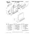
Nothing wrong with the manual or the delivery - came to me the same day I ordered it. But afterwards I realized that I ordered the wrong manual. Probably better with the Quick start - version. So maybe it would be better if we could see a list with inhold for each manual before ordering?
Pin No. 52 53 54 55 56 57 58 59 60 61 62 63 64 65 66 67 68 69 70 71 72 73 74 75 76 77 78 79 80 81 82 83 84 85 86 87 88 89 90 91 92 93
Pin Name TSTC TSTB TSTA TST2 TST1 TST0 DVCC DVCC AGND VRT1 VRTS1 AVCC Y IN VRBS1 VRB1 DGND DVCC AGND VRT2 VRTS2 AVCC U IN VRBS2 VRB2 DGND DVCC AGND VRT3 VRTS3 AVCC V IN VRBS3 VRB3 DGND DGND DVCC EVD EHD ECK EEVN MNT4 MNT3
I/O I I I I I I � � � I O � I O I � � � I O � I O I � � � I O � I O I � � � I I I I O O
Description
Input terminal for the test (normally: fixed at �L�)
Power supply terminal (+5V) (logic system) Power supply terminal (+5V) (A/D converter, digital system) Ground terminal (A/D converter, analog system) Reference voltage (top side) input of the A/D converter Reference voltage (top side) output of the A/D converter Generated 3V at connected to VRT1 (pin ^¡) Power supply terminal (+5V) (A/D converter, analog system) Analog Y signal input terminal (luminance signal input terminal) Reference voltage (bottom side) output of the A/D converter Generated 1V at connected to VRB1 (pin ^§) Reference voltage (bottom side) input of the A/D converter Ground terminal (A/D converter, digital system) Power supply terminal (+5V) (A/D converter, digital system) Ground terminal (A/D converter, analog system) Reference voltage (top side) input of the A/D converter Reference voltage (top side) output of the A/D converter Generated 3V at connected to VRT2 (pin &º) Power supply terminal (+5V) (A/D converter, analog system) Analog U signal input terminal (B-Y color difference signal input terminal) Reference voltage (bottom side) output of the A/D converter Generated 1V at connected to VRB2 (pin &�) Reference voltage (bottom side) input of the A/D converter Ground terminal (A/D converter, digital system) Power supply terminal (+5V) (A/D converter, digital system) Ground terminal (A/D converter, analog system) Reference voltage (top side) input of the A/D converter Reference voltage (top side) output of the A/D converter Generated 3V at connected to VRT3 (pin &ª) Power supply terminal (+5V) (A/D converter, analog system) Analog V signal input terminal (R-Y color difference signal input terminal) Reference voltage (bottom side) output of the A/D converter Generated 1V at connected to VRB3 (pin *¢) Reference voltage (bottom side) input of the A/D converter Ground terminal (A/D converter, digital system) Ground terminal (logic system) Power supply terminal (+5V) (logic system) Vertical drive data input from the CXD1229Q (IC401) Horizontal drive data input from the CXD1229Q (IC401) Serial clock signal input from the CXD1229Q (IC401) E/O input from the CXD1229Q (IC401) Test monitor output terminal (normally: open) Test monitor output terminal (normally: open)
5-60
|
|
|
> |
|